
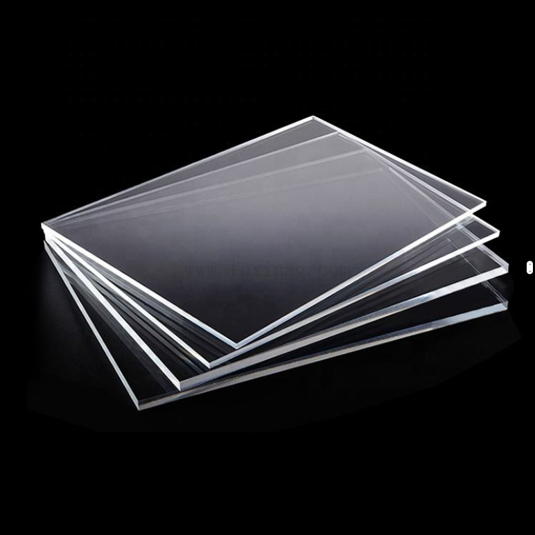
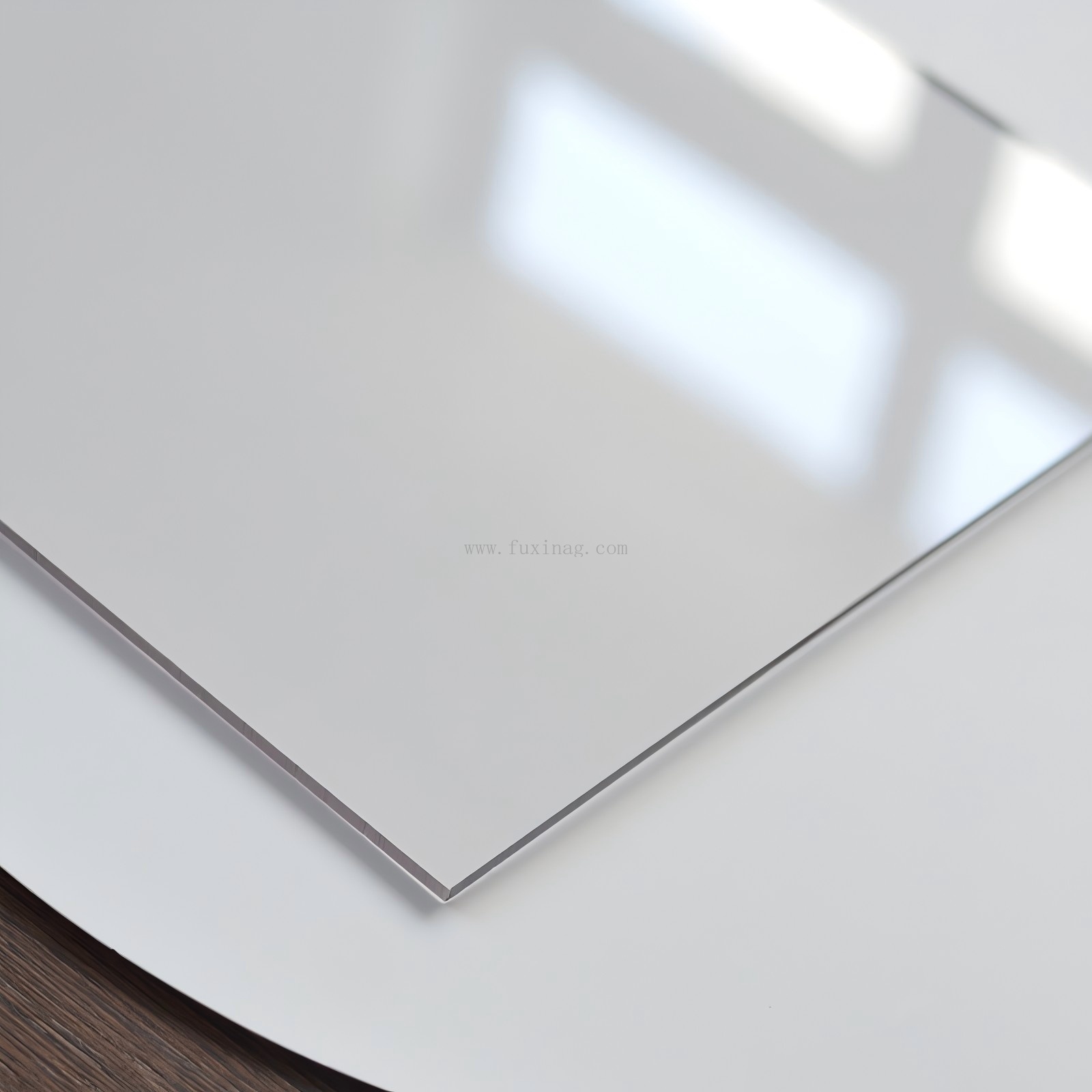
Glass Wafer Manufacturing Powering Next-Generation Semiconductors MEMS and Advanced Packaging
In the rapidly evolving semiconductor industry, glass wafers have emerged from specialized niches into a critical enabling material. High-purity glass wafers deliver exceptional dimensional stability, superior electrical insulation, optical transparency, and thermal performance that silicon and organic substrates cannot match in many applications. As demand surges for AI accelerators, high-bandwidth memory (HBM), CMOS image sensors (CIS), MEMS devices, and advanced packaging, glass wafer production is scaling rapidly to meet the needs of global electronics manufacturers.
Precision Manufacturing of Glass Wafers
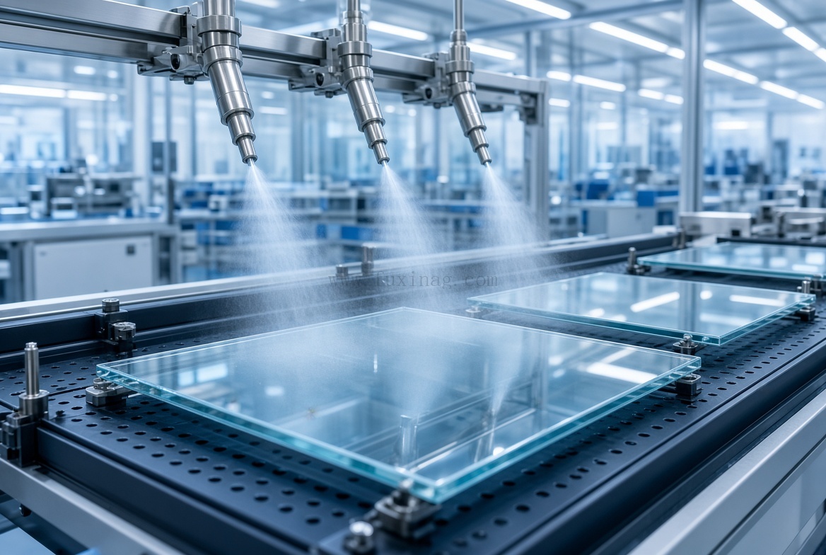
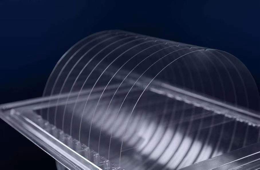
Producing semiconductor-grade glass wafers requires tightly controlled processes from raw material to finished substrate. High-purity silica or specialty glass compositions (borosilicate, fused silica/quartz, aluminosilicate, and low-CTE formulations) form the foundation. Common production routes include:
- Fusion draw processes that yield ultra-flat, pristine surfaces with minimal residual stress.
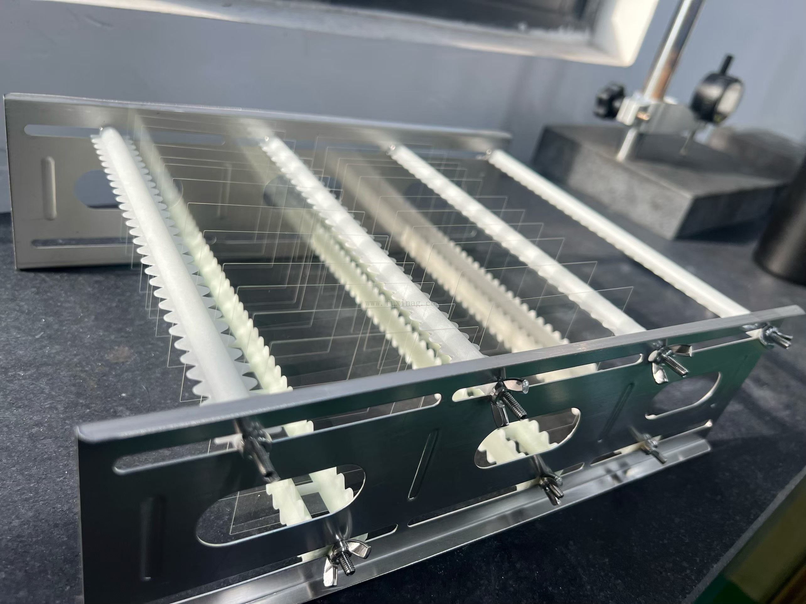
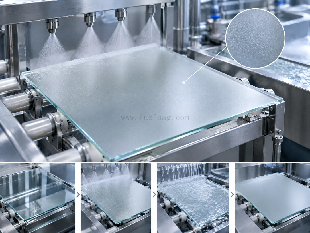
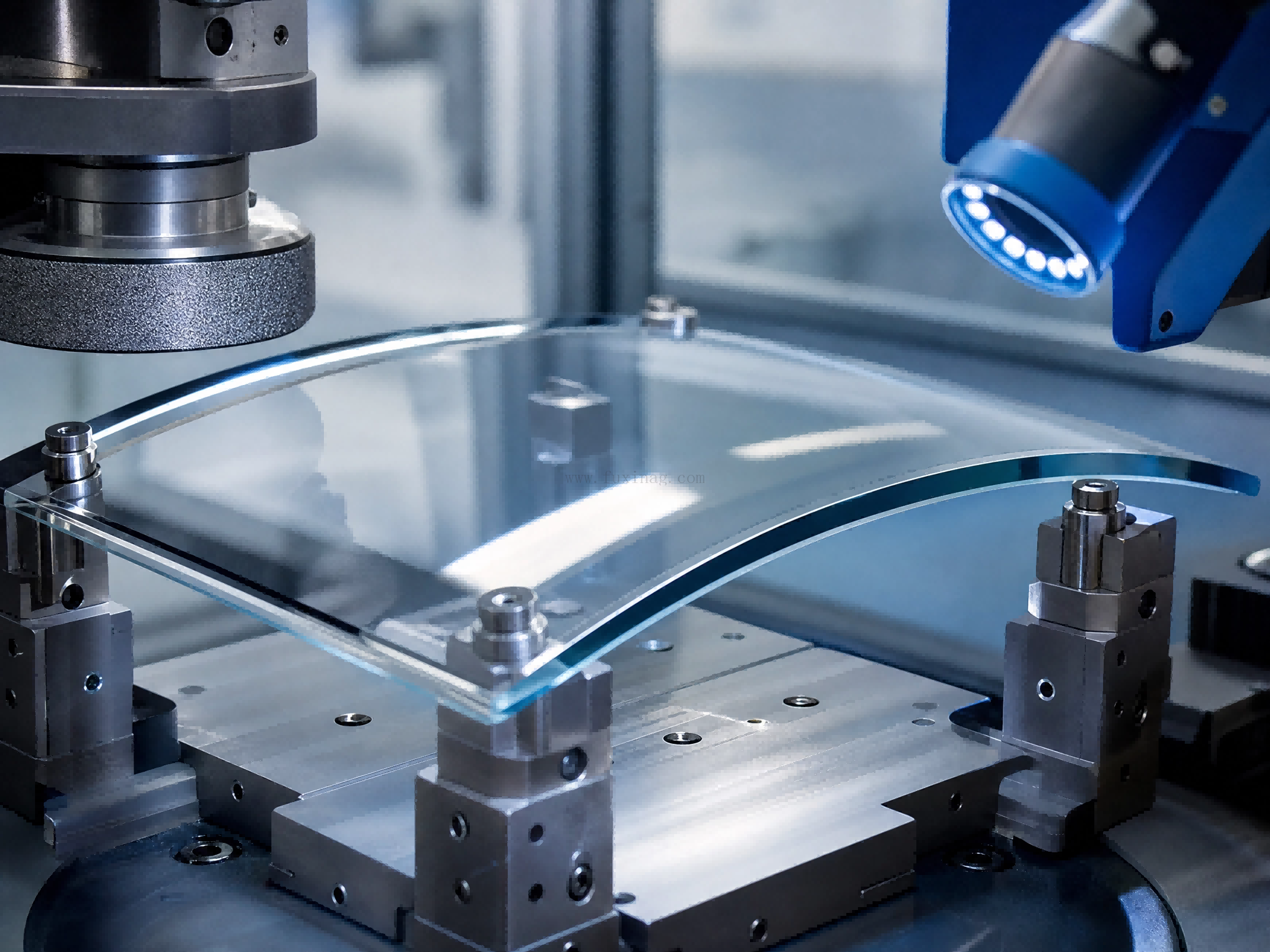
- Precision forming, annealing, grinding, and polishing to achieve tight thickness uniformity, total thickness variation (TTV), and surface roughness suitable for bonding and lithography.
- Advanced structuring, particularly Through-Glass Via (TGV) formation. The dominant industrial method combines femtosecond or picosecond laser induction with wet etching (or emerging plasma approaches) to create high-aspect-ratio vias that are later metallized, typically with copper.
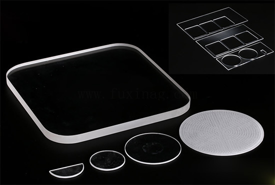
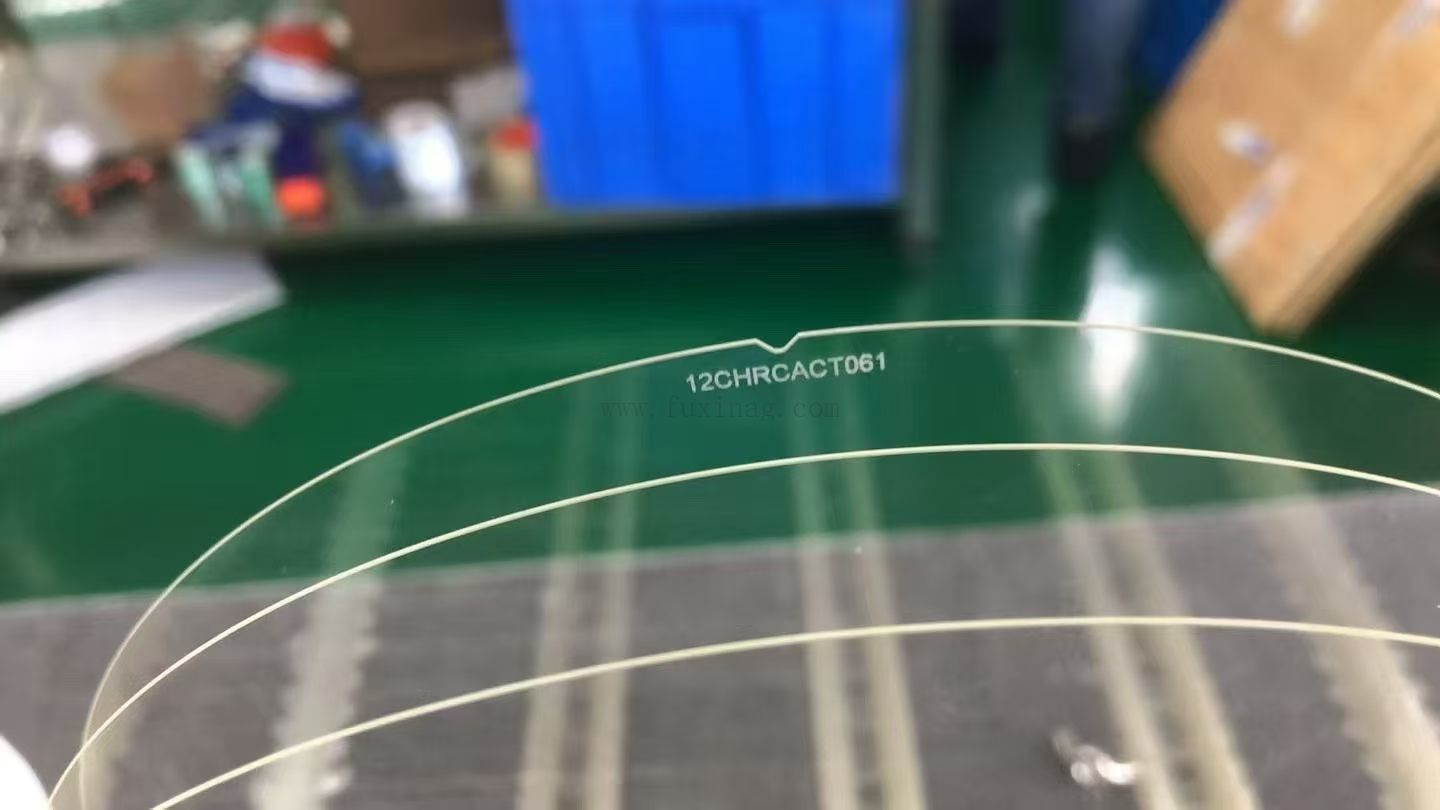
Finished wafers are available in standard diameters (100 mm, 150 mm, 200 mm, and increasingly 300 mm) as well as emerging panel formats. Carrier wafers, structured cavity wafers, interposers, and glass-core substrates each demand specific surface quality, CTE matching, and via density. Quality control emphasizes defect density, flatness, and hermeticity—critical for yield in downstream processes such as anodic bonding, temporary bonding, and 3D integration.
Key Properties Driving Adoption
Glass wafers offer a compelling combination of attributes:
- Low dielectric constant and low loss tangent for high-frequency RF and high-speed digital signals.
- Excellent optical transparency for CIS, photonics, and inspection.
- Chemical resistance and hermetic sealing capability ideal for MEMS and microfluidics.
- Superior mechanical rigidity and lower warpage compared with organic substrates, especially at larger package sizes and higher process temperatures.
- CTE options that can be tuned for silicon compatibility.
These properties enable higher interconnect density, better signal integrity, improved thermal management, and more reliable wafer-level packaging than traditional alternatives in many high-performance use cases.
Major Application Scenarios
Glass wafers serve diverse, high-growth segments:
- Advanced Packaging and Interposers: Glass core substrates and TGV interposers support multi-chiplet architectures, HBM integration, and large-body packages for AI/HPC processors. They reduce warpage, improve power delivery, and enable finer-pitch interconnects.
- CMOS Image Sensors (CIS): Still a dominant revenue driver; glass provides optical windows, carriers, and packaging elements.
- MEMS and Sensors: Cap wafers, cavity wafers, and anodically bonded structures for pressure, inertial, acoustic, and environmental sensors—widely used in automotive, consumer electronics, and industrial applications.
- Microfluidics and Bio-MEMS: Dimensional stability and chemical inertness support lab-on-chip and diagnostic devices.
- RF, Power, and Photonics: Low-loss substrates for RF modules, integrated passive devices, and photonic integrated circuits; transparency aids co-packaged optics.
- Emerging Uses: AR/VR optical elements, temporary carriers for wafer thinning and fan-out processes, and specialized power devices.
Asia-Pacific currently leads in both production and consumption, supported by a dense ecosystem of glass makers, substrate processors, and OSATs, while North America and Europe drive advanced R&D and high-end AI packaging demand.
Parter with Reliable Supplier
Are you looking for high-quality glass wafers or custom TGV substrates? Our factory specializes in precision glass wafer production for semiconductor, MEMS, CIS, and advanced packaging applications. Contact us for technical specifications, samples, or volume quotations to support your next-generation designs.